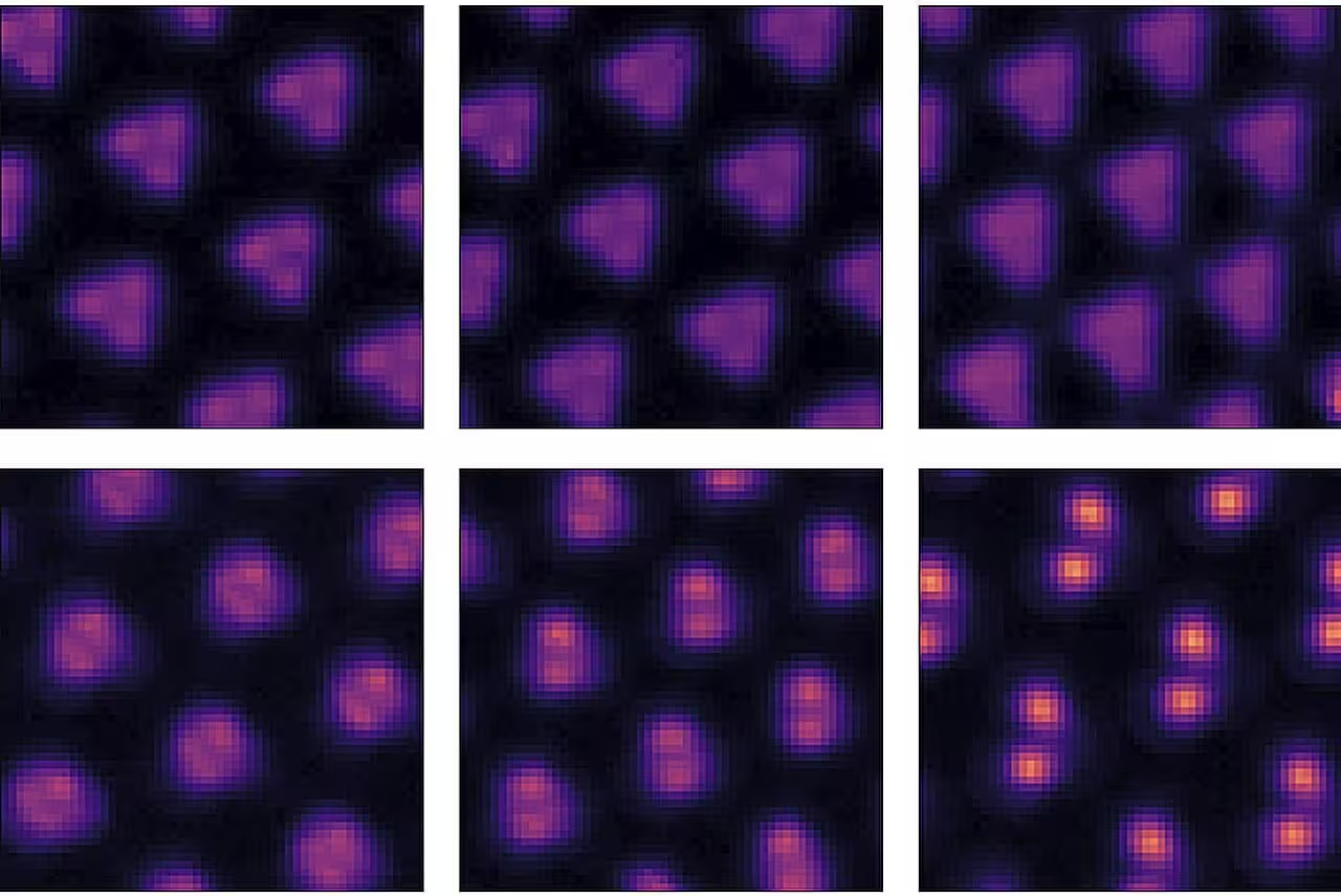
For a long time, scientists could not obtain an image of molecular electronic ice because the methods used destroyed the object of study. The same group that demonstrated the existence of the electron crystal invented a way to modify the scanning electron microscope and obtained the first images of the Wigner molecule.
Electrons often move so quickly through materials that they do not form bonds. In the 1930s, physicist Eugene Wigner (Eugene Wigner) predicted that electrons could be brought to a steady state at low densities and temperatures, forming “electron ice”, also known as a Wigner crystal.
In 2021, at Berkeley (USA), research groups led by Feng Wang (FengWang) and Michael Crommy (Michael Crommie) proved the existence of such electronic crystals. Now the same scientists have obtained an image of a new quantum phase of a solid electronic object – a molecular Wigner crystal. The results of the scientific study are published in the journal. Science.
Ordinary Wigner crystals form honeycombs with a regular arrangement of electrons. In molecular Wigner crystals, highly ordered structures are created from artificial “molecules” each consisting of two or more electrons.
For many years, scientists have attempted to obtain direct images of the molecular Wigner crystal. This turned out to be a difficult task because the molecular electron LED was destroyed when trying to photograph it. The tip of the scanning tunneling microscope (STM), which could be used to obtain the desired images, distorted the electronic configuration of the material.
In a new study, scientists from the Lawrence National Laboratory in Berkeley solved this problem. They developed a method that minimizes the electric field created by the STM tip. With the help of this modification, the researchers were able to capture the precise electronic structure of the molecular Wigner crystal.
For the experiments, scientists developed a nanomaterial called “twisted tungsten disulfide (tWS)”.2) moire type superlattice”. First, two-layer tungsten disulfide (WS2) with layers stacked on top of each other with a rotation angle of 58 degrees. They were deposited on 49-nanometer-thick hexagonal boron nitride (hBN) and a graphite gate.
Using STM techniques, physicists found that doping the tWS2 superlattice with electrons filled each 10-nanometer-wide cell with only two or three electrons. As a result, these packed cells formed a series of moiré-type electronic molecules across the superlattice, leading to the formation of a molecular Wignersky crystal.
“Low temperatures, together with the energy potential created by the tWS2 superlattice, trap electrons locally,” Wang explained.
In the future, Wang, Crommie and their team plan to apply STM techniques to study this new quantum phase more deeply and find the possible applications it could open.
Source: Port Altele
